| Japanese | English |
Design Specification
1. Noise Cancelling Algorithm[1]1-1. Specter Subtraction Method (SS Method)
1-2. MAP method using Variable Speech Distribution
1-2-1. MAP Estimate Method
1-2-2. Speech spectrum distribution proposed by T.Lotter and P.Vary
1-2-3. Variable Speech Distribution
2. Implementation of the Noise Cancelling System
2-1.Separating into the Hardware and the Software
2-1-1.Features of the HW and the SW
2-1-2. Feature of Noise Cancelling System
2-1-3. Architecture
2-2. Hardware
2-2-1. Processing flow
2-2-2. Circuit structure
2-2-3. HW timing
2-3. Software
2-3-1. Source code
2-3-2. Flow chart
3. Development Environment
3-1. Hardware Design Process
3-1-1. Design Hardware Logic
3-1-2. Manual of Xilinx ISE and EDK
3-2. Software design process
4. Contest Design Target
5. SPEED and AREA
6. References
7. Download
17th LSI Design Contests・in Okinawa Design Specification - 2-2
2-2. Hardware
In this chapter, we describe processing flow using hardware. In addition to this chapter, chapter 2-3 (Software) helps your understanding of processing flow of hardware.
2-2-1. Processing flow
1. CPU imports Sample data from AC97.
2. CPU outputs the data into Window Filtering every 1 sample data. FIFO1A and FIFO1B store them every
64 samples data.
Then, FIFO1A stores for 32 samples data earlier than FIFO1B as follows.
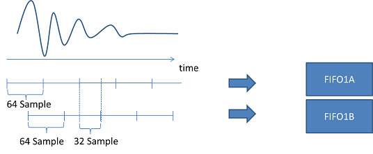
Figure 7
3. When 64 samples data are stored in FIFO1A or FIFO1B, the data are output into FFT circuit.
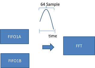
Figure 8
4. FIFO2 stores the data after FFT processing. (FIFO2_Re stores real part of the data. FIFO2_Im stores
imaginary part of the data.)
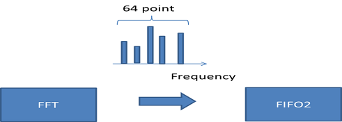
Figure 9
5. CPU imports the data from FIFO2.

Figure 10
6. CPU outputs the data into FIFO3. (FIFO3_Re stores the data that input into real part of the FFT circuit.
FIFO3_Im stores the data that input into imaginary part of the FFT circuit.).

Figure 11
7. When 64 points data are stored in FIFO3, the data are output into FFT circuit and processed by IFFT.
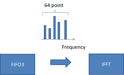
Figure 12
8. After IFFT processing, the data are stored in FIFO4A or FIFO4B. The data from FIFO1A are stored in
FIFO4A and the data from FIFO1B are stored in FIFO4B.

Figure 13
9.When 64 samples data are stored in FIFO4A or FIFO4B, 32 samples data are stored in the other. 32
samples data are taken out from FIFO4A and FIFO4B, and the data are stored in FIFO5 after Half
Overlap processing.
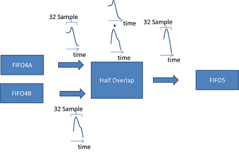
Figure 14
10. CPU imports the data from FIFO5.
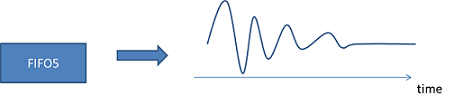
Figure 15
11. CPU outputs the data into AC97.
2-2-2. Circuit structure
The circuit structure is shown by figure 16.

Figure 16
2-2-3. HW timing
The timing chart is shown by figure 16. The number in the row of FIFO expresses the number of the sample point of the data in the FIFO.
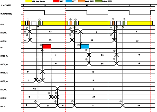
図17