Design Specification
1.Small RISC Processor
(SRP) architecture
5.Instruction ROM and
Data Memory
BASIC
FREE
12th LSI Design Contests・in Okinawa Design Specification - 5
5.Instruction ROM and Data Memory
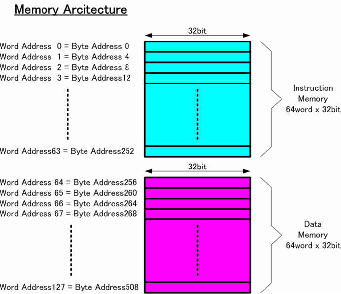
Two memories are explained in figure 1. In order to run the given sorting program in SRP, following memory configurations are assumed (figure 4).
The instruction memory is assumed to be Read Only Memory (ROM). The size is 64 word x 32 bits, then 256 bytes memory. 0 to 255 byte addresses are assigned for Instruction memory.
The data memory also have the same size such as 64 word x 32 bits = 256 bytes. 256 to 511 byte addresses are assigned for Data memory.
Byte address more than 512 is NOT used.

Figure 4 Memory Organaization
6.VHDL CODES
In order to verify your HDL of SRP, sorting program is given. The VHDL codes is also provided. If you use other than VHDL, please prepare similar environment by yourself.
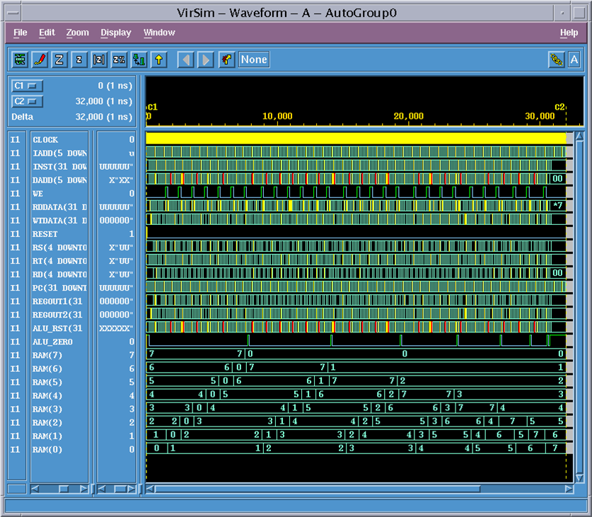
In the given VHDL, 8 words BUBBLE sorting algorithm is implemented. The instruction ROM for the BUBBLE sort code and Data RAM with initial values are provided.
After the de-assertion of Reset signal, program counter starts from address=0.
Please monitor the DATA memory contents such as figure 5.
packagealu_pkg.vhd
Instruction ROMirom.vhd
Data RAMdram.vhd
SRP templateSRP.vhd
Test benchtest_SRP.vhd

Figure 5 Bubble sorting simulation waveform example
