
Design Specification
1.Small RISC Processor
(SRP) architecture
5.Instruction ROM and
Data Memory
BASIC
FREE
12th LSI Design Contests・in Okinawa Design Specification - 8
9.SRP design example
In this section, one design example of SRP is explained as shown in figure 7. One instruction per one cycle operation is assumed.
Instruction ROM is also assumed to output one instruction according to word address input signal.
Register file uses ra1 and ra2 register address input signals. According to ra1 and ra2, register file outputs data to do1 port and do2 port respectively. The wa is address signal for write register file location and the written data is inputted to din port. When writer signal is asserted (=1), the data will be written at Clock rising edge.
Instructions which needs to write data into register file are add, sub, and, or, lw, slt as summarized in Table 7.
Table 7: How many data access to register file for each instruction
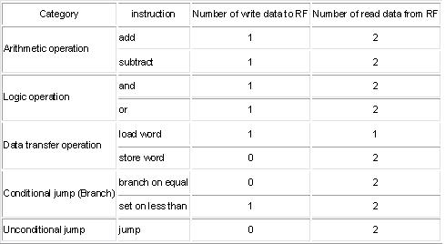
ALU does the operation of add, sub, and, or. In addition, ALU check the its output (result) is zero or not (zero). For slt operation, ALU performs subtraction and by checking zero-flag, slt can be implemented.
Instruction sw needs data memory write operation and instruction lw needs data memory read operation.
In figure 7, triangle mark indicates Clock inputs. At only Clock rising edge, all flip-flop data update are performed. Then the circuit block without the triangle mark is combinational logic circuits.
“&” means bit concatenation. “+” means adder. “MUX” means multiplexer. “SE” is the 16 bits to 32 bit expansion with sign bit. Table 8 shows the more explanation of this sign-extend bit expansion. As you see form the table, just MSB is copied 16 times.
Table 8: sign-extended 16bits to 32bits expansion
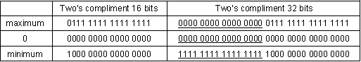
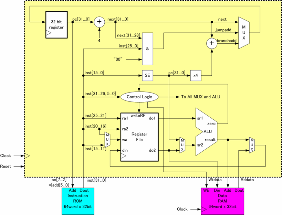
Figure 7: SRP design example
Right upper 3 inputs MUX in figure 7 is for Program Counter. If signal next is selected, PC will increment by 4, else signal jumpadd is selected, unconditional Jump happened, else signal branchadd is selected, branch is taken.
For signal jumpadd generation, “&”, that is, concatenation is used. Concatenation of LSB “00” corresponds to two bit left shift, that is, 4 time multiply.
The signal branchadd is corresponds to PC+4+offset*4.
Figure 8 shows that 3 cycle operations of some signals in figure 4. Instruction ROM address Iadd is generated from PC, then instruction “inst” comes out from the ROM. According the field of inst, ra1, ra2, wa are generated.
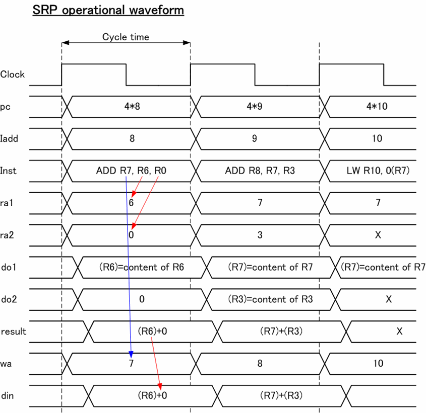
Figure 8: SRP operational waveform