| Japanese | English |
15th LSI Design Contests・in Okinawa Design Specification - 4-2-2
4-2-2. FFT circuit : N=8
(1) Circuit design
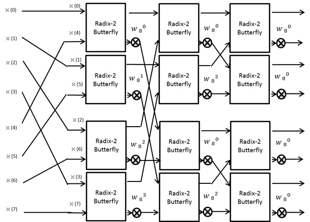
Figure 15: The block diagram of 8-point FFT circuit for parallel input signal
Figure 26: The block diagram of 8-point FFT circuit for serial input signal
First, the way of 8-point FFT circuit design is explained as follow.
This architecture inputs serial input signal to butterfly operation circuit. The output signals of butterfly operation circuit are selected to compute next butterfly operation by multiplexer.
This circuit is shown in figure 27.
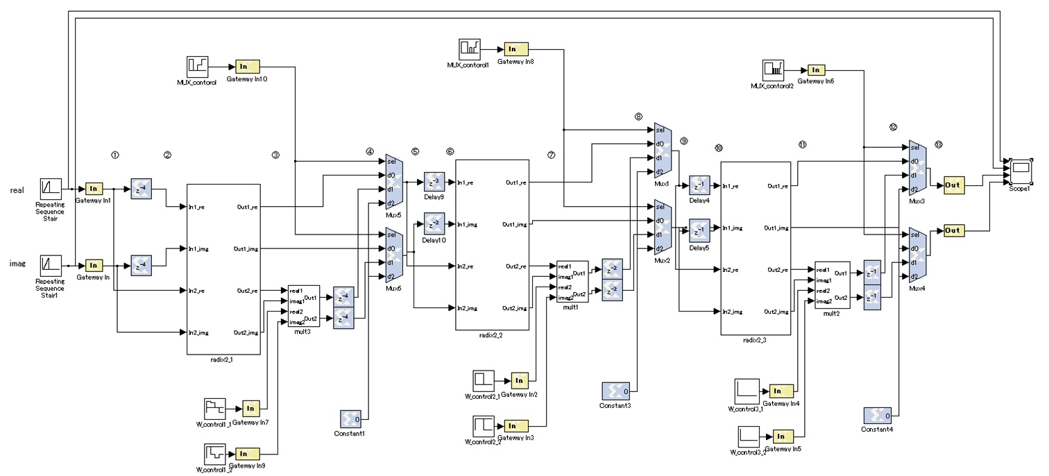
Figure 27: 8-point FFT circuit to the serial input
a) MUX_control
The MUX_control block is a sequence that controls the signal input to the selector of the multiplexer. This signals that determine the output of the multiplexer.
In figure 28, we shows the parameter of sequence.
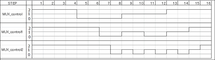
Figure 28: Parameters of the MUX_control sequence
In figure 28, we confirmed that MUX_control value output from each step has been changed. Only the signals required for the FFT butterfly computation circuit of output signal is controlled sent to the next butterfly computation circuit.
b) W_control
W_control is a sequence represented the rotation factor W
By varying the value of the complex twiddle factors are multiplied per STEP, butterfly computation is performed.
The complex twiddle factor is
![]() ,
,
![]() ,
,
![]() ,
,
![]() In Table 7, we shows the parameter of sequence.
In Table 7, we shows the parameter of sequence.
Table 7: Parameters of the W_control sequence
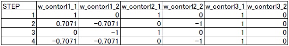
In Table 7, we used the
![]() is as approximate number 0.7071.
is as approximate number 0.7071.
In Tabel 7, we confirmed multiply the first step in
![]() ,
in MULT0 of the figure 26, since then, in turn multiplied by
,
in MULT0 of the figure 26, since then, in turn multiplied by
![]() ,
,
![]() ,
,
![]() ,
The first step in MULT1 multiplies the
,
The first step in MULT1 multiplies the
![]() the next step is to multiply the
the next step is to multiply the
![]() The MULT2 are always multiplied by the
The MULT2 are always multiplied by the
![]()
In figure 27, we show the 8-point FFT circuit timing chart of figure 29 for the serial input.
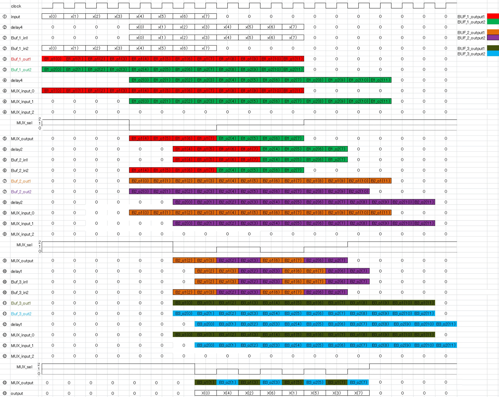
Figure 29: 8-point FFT circuit timing chart for the serial input
(2) Evaluation
Because it is hard to recognize the value of under decimal point from output wave shown by figure 26, we show those values on MATLAB. x(0)=0+0j, x(1)=1+1j, x(2)=2+2j, x(3)=3+3j, x(4)=4+4j, x(5)=5+5j, x(6)=6+6j, x(7)=7+7j Output signals are
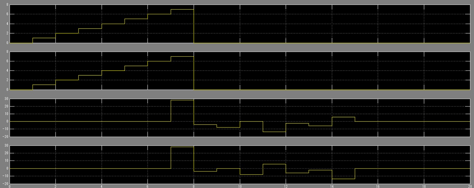
Figure 30: 8-point FFT circuit on the output signal of the serial input
In Figure 30, as will be noted from the Table 8, first step on MULT0 is multiplying by X(0)=28+28j, X(1)=-13.6570+5.6575j, X(2)=-8+0j, X(3)=-5.6570-2.3430j, X(4)=-4-4j, X(5)=-2.3430-5.6575j, X(6)=0-8j, X(7)=5.6570-13.6570j
The deference between above values and the results calculated on MATLAB (Figure 27) is shown by table 8.
Maximum error is,
![]() A reason of this error is Round-off Error caused by representing
A reason of this error is Round-off Error caused by representing ![]() with binary .
with binary .
Table 8: Error compared to calculated results on MATLAB
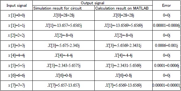

Figure 31:&Calculated results on MATLAB