| Japanese | English |
15th LSI Design Contests・in Okinawa Design Specification - 4-2-3
4-2-3. FFT circuit : N=16
(1) Circuit design
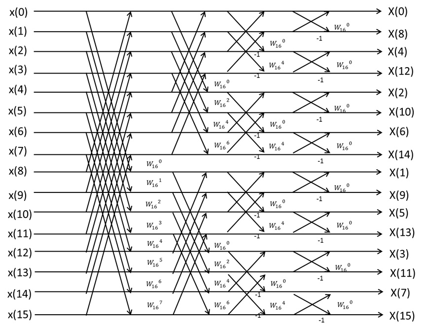
Figure 32: 16 points FFT architecture
Figure 33: Block diagram of 16 points FFT architecture for serial input
A serial input signal is delayed and carried into Butterfly arithmetic circuit. Then, system separates output signals of Butterfly processing circuit into required signals for calculating FFT and no required signals by using Multiplexer.
After that, required signals are carried into next Butterfly arithmetic circuit. A circuit which we have made is shown by figure 34.
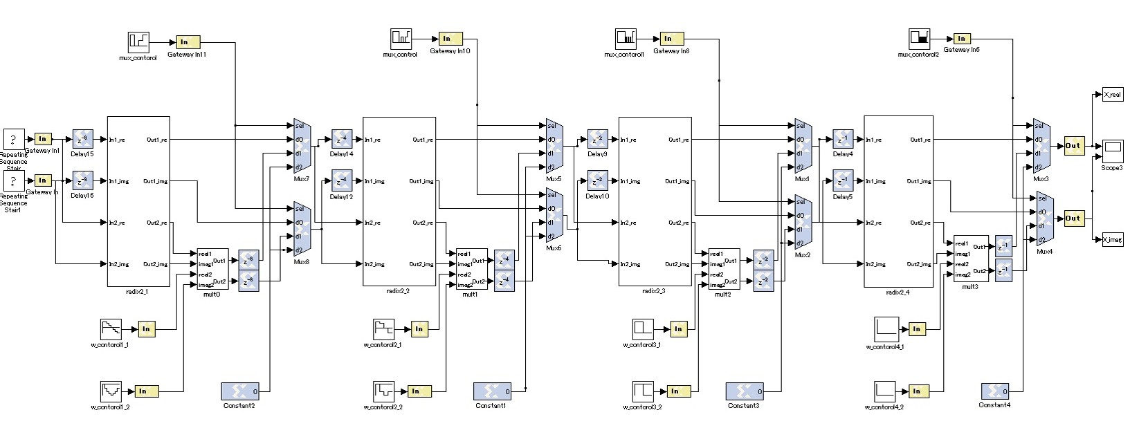
Figure 34: 16 points FFT circuit for serial input
1) MUX_control
MUX Control block controls input signal carried into selector of multiplexer. Output signal of Multiplexer is decided by this control.
The sequence parameter is shown by figure 35.
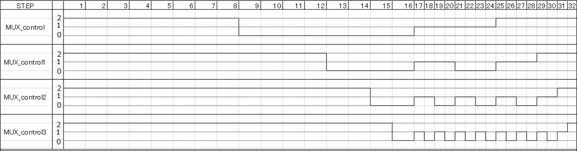
Figure 35: MUX_control sequence parameter
In figure 35, output signal from MUX_control varies on each step. The only signals required for FFT are sent to next Butterfly arithmetic circuit by the signal varying.
2) W_control
W_control is sequence representing twiddle factor W.
Butterfly arithmetic is done by varying W complex multiplied on each step.
Each W are…![]() ,
,
![]() ,
,
![]() ,
,
![]() ,
,
![]() ,
,
![]() ,
,
![]() ,
,
![]() Sequence parameters are shown by table 9.
Sequence parameters are shown by table 9.
Table 9: W_control sequence parameter
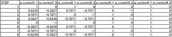
In Table 9,
![]() is expressed as 0.7071,
is expressed as 0.7071,
![]() is expressed as 0.9239 and
is expressed as 0.9239 and
![]() is expressed as 0.3827.
is expressed as 0.3827.
In Figure 30, as will be noted from the Table 9, first step on MULT0 is multiplying by
![]() and the next steps are multiplying by
and the next steps are multiplying by
![]() ,
,
![]() ,
,
![]() ,
,
![]() ,
,
![]() ,
,
![]() ,
,
![]() in order. First step on MULT1 is multiplying by
in order. First step on MULT1 is multiplying by
![]() and the next steps are multiplying by
and the next steps are multiplying by
![]()
![]()
![]() in order. First step on MULT2 is multiplying by
in order. First step on MULT2 is multiplying by
![]() and the next step are multiplying by
and the next step are multiplying by
![]() All steps on MULT3 is multiplying by
All steps on MULT3 is multiplying by
![]()
Timing diagram of 16-points FFT circuit for serial input is shown in Figure 36.
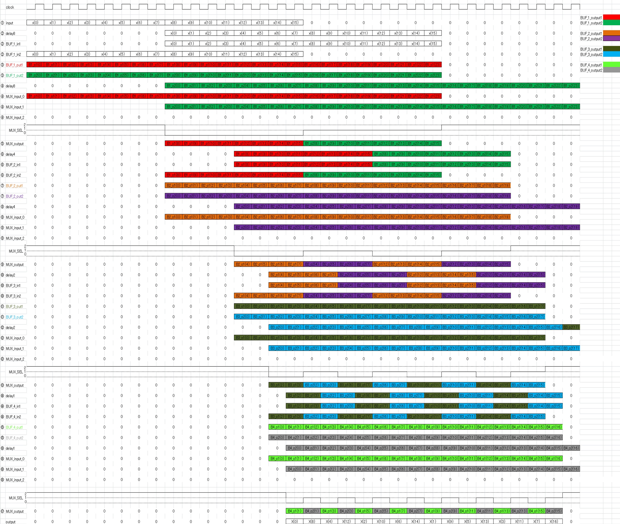
Figure 36: Timing diagram of 16-points FFT circuit for serial input
(2) Verification
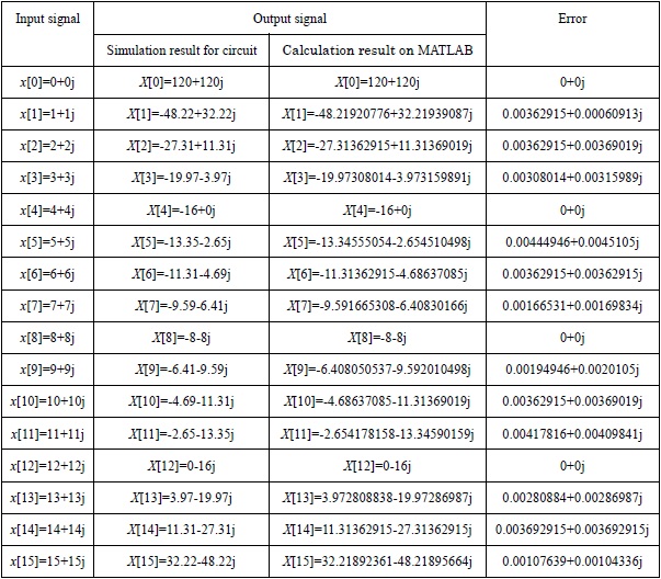
A simulation result for input signals that x(0)=0+0j, x(1)=1+1j, x(2)=2+2j, x(3)=3+3j, x(4)=4+4j, x(5)=5+5j, x(6)=6+6j, x(7)=7+7j, x(8)=8+8j, x(9)=9+9j, x(10)=10+10j, x(11)=11+11j, x(12)=12+12j, x(13)=13+13j, x(14)=14+14j, x(15)=15+15j is shown in Figure 37.
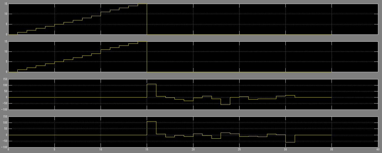
Figure 37:
Calculation results on MATLAB and the errors are shown in Table 10.
Figure 10: Output waveform of 16-points FFT circuit for serial input
By Figure 37, the Latency between an input and an output for this circuit is 15.
The verification of 16-points FFT circuit is making m-file for test, and calculation of mean square error (MSE) between result on MATLAB and result for circuit by random inputs a hundred times. The result is shown in Table 11.
Table 11: Calculation result of MSE
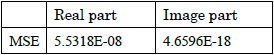
By the Verification, this 16-points FFT circuit perform that MSE of real part is
 、
and image part is
、
and image part is
![]()