| Japanese | English |
15th LSI Design Contests・in Okinawa Design Specification - 4-2-1
4-2-1. Design of FFT circuit for serial input
(1) Circuit design in the case of N=4
In chapter A-1, we designed 4 point FFT circuit for parallel input.
The FFT circuit for parallel input can be designed easily, and it has an advantage that Input to Output latency is 0. However the circuit scale becomes very large.
If we designed FFT circuit with less butterfly circuits by reusing them with delay blocks and multiplexer (MUX) blocks, we could make the circuit scale smaller.
In this chapter, we design 4 point FFT circuit for serial input.
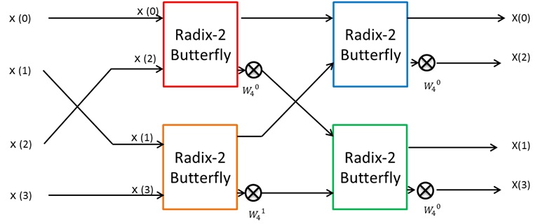
Figure 17: 4 point FFT circuit for parallel input
The conceptual block diagram is as follows.
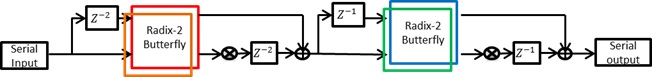
Figure 18: Block diagram of 4 point FFT circuit for serial input.
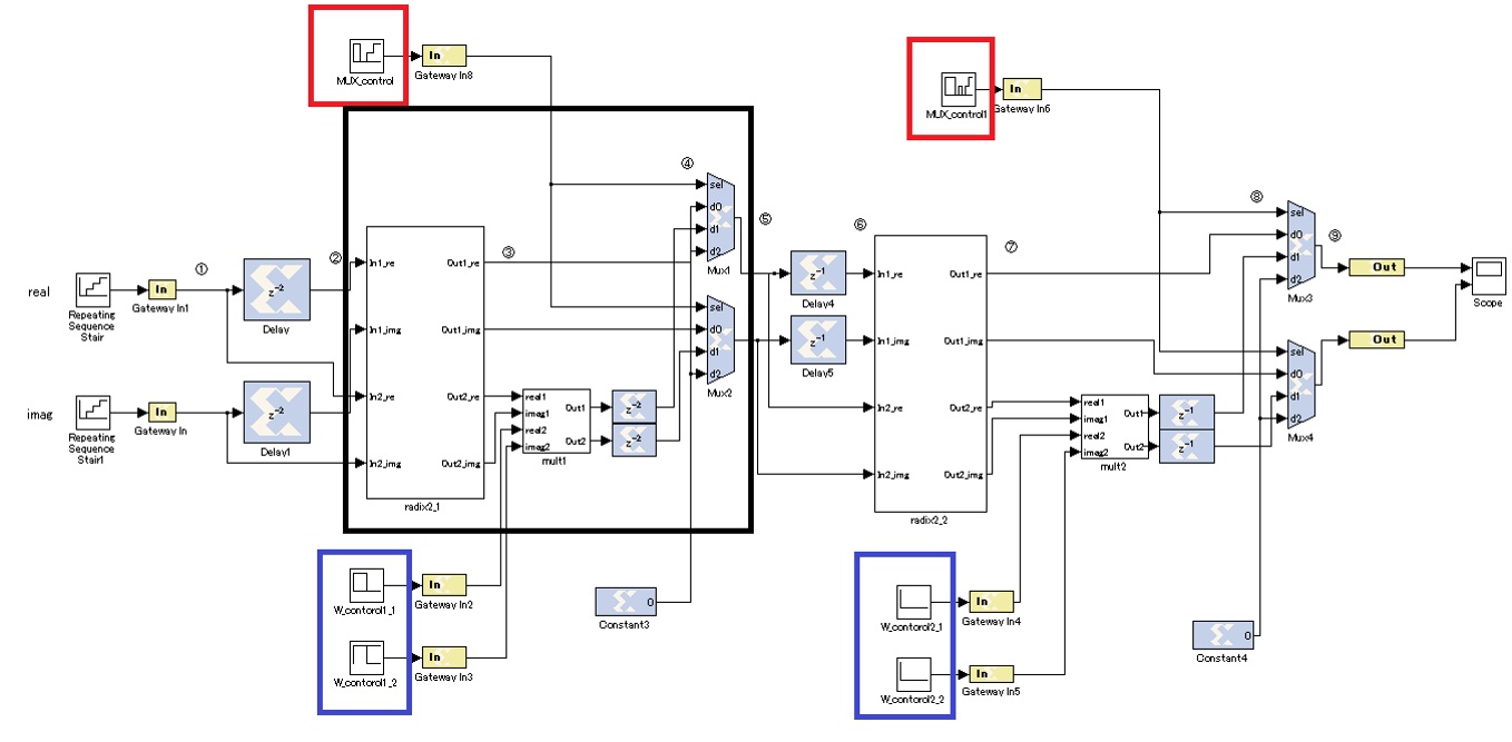
Figure 19: 4 point FFT circuit for serial input
The details of MUX_control and W_control blocks in Figure 19 is described as follows.
a) MUX_control

Figure 20: Enlarged view around MUX_control
MUX1 and MUX2 output the values of d0 ~ d2 when sel=0~2. MUX_control decides the output signal of MUX1 and MUX2 multiplexers from d0 ~ d2
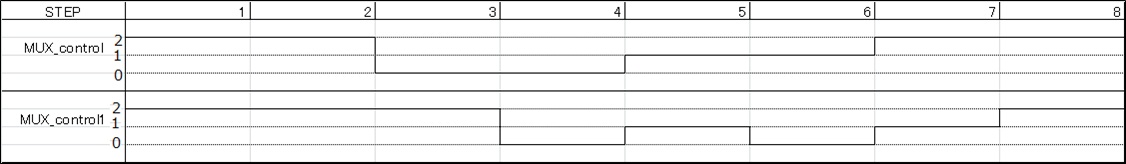
Figure 21: The chart of MUX_contol
The output signal of MUX_control is variable at each step. Therefore, MUX_control can select the signal which is input to next butterfly circuit.
b) W_control
W_control decides the twiddle factor W.
This architecture computes butterfly operation changing the value of twiddle factor W (real part, imaginary part) at each step.
Each block parameters are shown in Table 5.
Table 5: W_control block paramters
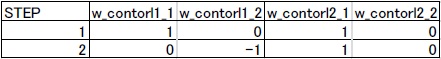
From this table, MULT1 block operates multiply by ![]() at first step and
at first step and ![]() at next step.
MULT2 block always operates multiply by
at next step.
MULT2 block always operates multiply by ![]()
The timing chart of 4-points FFT circuit for serial input signal is shown in Fig. 22.
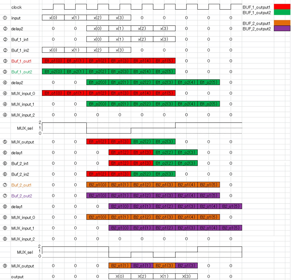
Figure 23: The timing chart of 4-points FFT circuit for serial input signal
(2) Verification
simulation result of this architecture using x(0)=0+0j, x (1)=1+1j, x(2)=2+2j, x(3)=3+3j as input signal is shown in Fig. 23.
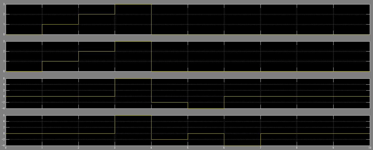
Figure 24: The output signal of 4-point FFT circuit for serial input signal
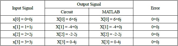
From this figure, the output signal of this architecture is X(0)=6+6i, X(1)=-4+0i, X(2)=-2-2i, X(3)=0-4i which is same as the MATLAB simulation result (Table 6).
Table 6: The comparison between circuit and MATLAB
And latency of this architecture is 3 clocks.
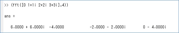
Figure 25: MATLAB simulation result