| Japanese | English |
14th LSI Design Contests・in Okinawa Design Specification - 8
8.Level 1 Basic Task
In this level, designer needs to design compression and decompression system as shown in Figure 11. The input of the system is QCIF size image (176 x 144 pixels). The input image is divided into 8x8 pixels which are called a block data of Y, Cr and Cb. The processing is done in raster scan manner that is started from upper left, and end in lower right corner of the image. The compression module consists of blocks as defined in Figure 12. The 1D-DCT block uses architecture as defined in Figure 5.
For each block of data processing, complete timing diagram is illustrated in Figure 13. The input data enters the compression module in column wise (C0, C1…C7). Each column consists of 8 pixels data with different row (R0, R1…R7). Therefore 8 clock cycles are required to input all block data. The input signal coming serially indicated by valid_input signal. One clock cycle after the first column data C0, the signed output is come out of Unsigned to Signed processing block. Therefore this block processing latency (Lsigned) is one clock cycle.
The output of Unsigned to Signed processing block is feed into 1D-DCT processing block. The processing latency (L1D-DCT) depends on how 1D-DCT in Figure 5 is implemented. The designer may divide it into several pipeline stages. The output of 1D-DCT processing block is stored in Transposition Buffer.
After all one block of pixels are processed by 1D-DCT processing block, the result is processed again by 1D-DCT in different direction. The processing delay is still the same with L1D-DCT. As soon as the first column data is finished, the result is computed by the Quantizer processing block. The latency of Quantizer processing (LQUANT)depends on how to implement it and its bit width. As a result, total time required to process a block of pixels data depends on Lsigned, L1D-DCT, and LQUANT.
The signed, transformation and quantization process are held when enable signal is asserted. Enable signal indicates that the core is ready to receive new input data. After some latency, output signal is validated when valid_output signal is asserted.
In order to optimize the design parameter (size, speed) while maintaining the image quality, the designer has to decide the optimum bit width of each processing block. This can be done by simulating the processing using fix point representation.
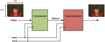
fig11 System Organization
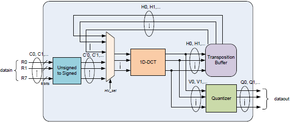
fig12 The Compression Module Block Diagram
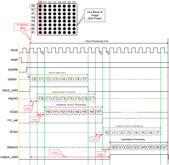
fig13 One Block Compression Timing Diagram
| No | Name Port | Description | Active | I/O | Width |
| 1 | clock | Clock signal | Input | 1 | |
| 2 | reset | Reset signal | Low | Input | 1 |
| 3 | enable | Indicates that the core is ready to receive new data | High | Input | 1 |
| 4 | cmode | Table quantization selector (Q50=0,Q80=1) | Input | 1 | |
| 5 | datain | Column input signal | Input | 64 | |
| 6 | valid_input | Sample the valid data at datain port | High | Input | 1 |
| 7 | valid_output | Validata the output data at dataout port | High | Output | 1 |
| 8 | dataout | Compressed image signal | Output | 64 |
Table2 Port Definition